The Quiet Reshaping of the AI Chip Supply Chain
Structural transformation of the AI chip supply chain, analyzing hard data from TSMC, ASML, and Micron to demonstrate how advanced packaging (CoWoS) and high-bandwidth memory have become the ultimate bottlenecks of the global tech economy.
3 min read · San Francisco, USA
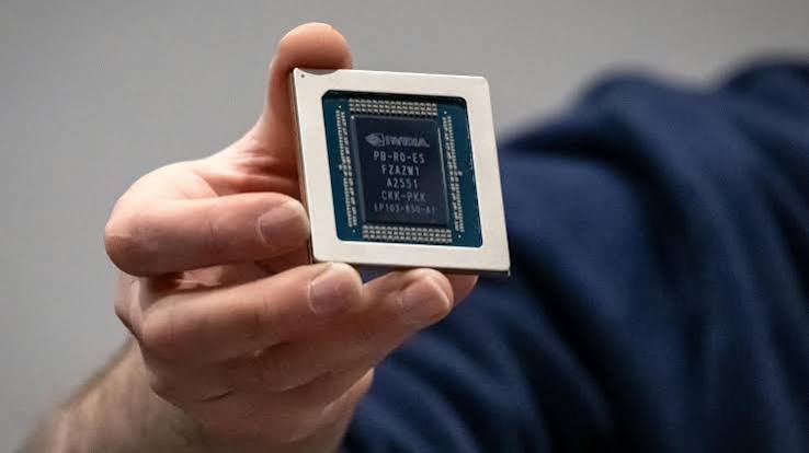
Public narrative surrounding the artificial intelligence boom has been fixed on software: foundational model parameters, context windows, and multi-billion-dollar corporate turf wars. But beneath the surface of soaring stock valuations and generative breakthroughs lies a vastly different theatre of conflict—one fought not with code, but with extreme ultraviolet light, micro-meter precision, and atomic-scale packaging.
The AI hardware narrative is rarely about who builds the cleverest model anymore. It is about who controls the choke points of the physical manufacturing apparatus.
As hyperscale cloud providers ramp capital expenditures to unprecedented heights, the global semiconductor supply chain has undergone a quiet, radical restructuring. The bottlenecks have shifted away from raw silicon mining and toward three hyper-specialized nodes: lithography equipment, advanced foundry processing, and high-bandwidth memory integration.
Layer 1: The Lithography Choke Point
At the absolute genesis of every high-performance AI accelerator sits ASML, the Dutch monopoly producer of Extreme Ultraviolet (EUV) lithography systems. Without these multi-hundred-million-dollar machines, printing sub-3-nanometer circuitry is a physical impossibility.
Recent operational disclosures and market trackers reveal that ASML’s capacity has become a master barometer for total industry growth. With full-year 2026 sales guidance tracking between 43 billion and 45 billion euros, the company’s advanced Low-NA and emerging High-NA systems are fully allocated well in advance.
ASML and Foundry Production Capacity Trajectory (2025-2026)
---------------------------------------------------------------------------------
System / Metric 2025 Baseline 2026 / 2027 Projected
---------------------------------------------------------------------------------
ASML EUV Shipments (Low/High-NA) ~65 Systems +30% YoY expansion ramp
TSMC Quarterly Revenue Run-Rate ~$25.6 Billion ~$40.2 Billion (Q2 peak)
TSMC Advanced Node Share (N3/N2) ~60% of Wafer Revenue 77% of Wafer Revenue
---------------------------------------------------------------------------------
*(Sources: Compiled from ASML quarterly reports, TSMC investor disclosures, and DataPorium industry audits.)*
Layer 2: The Foundry and Packaging Bottleneck
If lithography is the printing press, Taiwan Semiconductor Manufacturing Company (TSMC) is the sole printing house capable of executing high-volume production for top-tier AI architecture.
However, the true structural ceiling of the AI hardware boom is no longer just front-end wafer fabrication—it is advanced packaging. Chips like Nvidia’s Blackwell architectures and custom Google or Meta ASICs cannot function as monolithic dies; they require Chip-on-Wafer-on-Substrate (CoWoS) packaging to bridge logic dice directly with memory stacks.
As of mid-2026, TSMC’s CoWoS and CoWoS-L packaging lines remain completely booked out, with lead times stretching from 52 to 78 weeks. Even as TSMC pushes monthly capacity toward nearly 90,000 wafers, demand from hyperscalers continues to outpace supply by a wide margin. This has forced a diversification wave, pushing overflow orders into outsourced semiconductor assembly and test (OSAT) providers like Amkor and regional foundries, though lead times across alternatives remain heavily constrained.
Layer 3: The High-Bandwidth Memory (HBM) Multiplier
An AI processor starved of data bandwidth is a Ferrari idling in neutral. This reality has turned High-Bandwidth Memory (HBM) into the most lucrative, fiercely contested real estate in modern electronics.
The financial performance of memory leaders underscores this structural shift. Micron Technology reported fiscal third-quarter results showcasing revenue surging past $41.4 billion—more than quadrupling year-over-year—bolstered by an astonishing 84.6% gross margin driven almost entirely by the HBM shortage. With SK Hynix, Micron, and Samsung locking down multi-year allocations for HBM3E and early HBM4 ramps, acquiring memory capacity has become a board-level prerequisite before a company can even reserve a foundry slot.
The Strategic Re-Alignment
The implications of this supply-chain architecture are profound. Because lead times for leading-edge nodes like TSMC’s N2 (2nm) stretch up to 156 weeks into 2028, market entry is effectively restricted to entities with multi-year capital visibility. Smaller startups can no longer easily spin up custom silicon prototypes without colliding with massive, pre-booked orders from tech giants like Microsoft, Amazon, Google, and Meta, whose combined capital expenditure projections eclipse $725 billion.
The AI revolution is ultimately bounded not by human imagination, but by the physical yield of silicon wafers, the availability of Dutch optical systems, and the microscopic precision of stacking memory on logic. The supply chain has not broken; rather, it has consolidated into the most complex industrial pipeline in human history.
Watch
Sources
Technology reporter. AI, chips, platforms and the people building them.
Comments (0)
Comments are turned off for this story.